Our Global Impact 

Pozzetta serves industry-leading clients across the globe, with semiconductor device fabrication customers found in Australia, Germany, Italy, France, Sweden, Japan, and beyond.

1,400 products

1,300 active customers 

35 countries served 

3,500 annual shipments

About Us
semiconductor device fabrication

How we’ve helped our global clients

The world of semiconductor device fabrication is complex and ever-changing, which is why we believe it is absolutely critical to always provide customized, attentive support to our clients as they resolve their optimization issues. Here are a few ways we’ve definitively improved our clients’ processes with our custom solutions

Marcus Pozzetta
President

“Our customer was experiencing particle contamination on their photomasks. We solved this problem by designing a new latch that generated fewer particles during their production process.”

Scott Reese
ACCOUNT EXECUTIVE

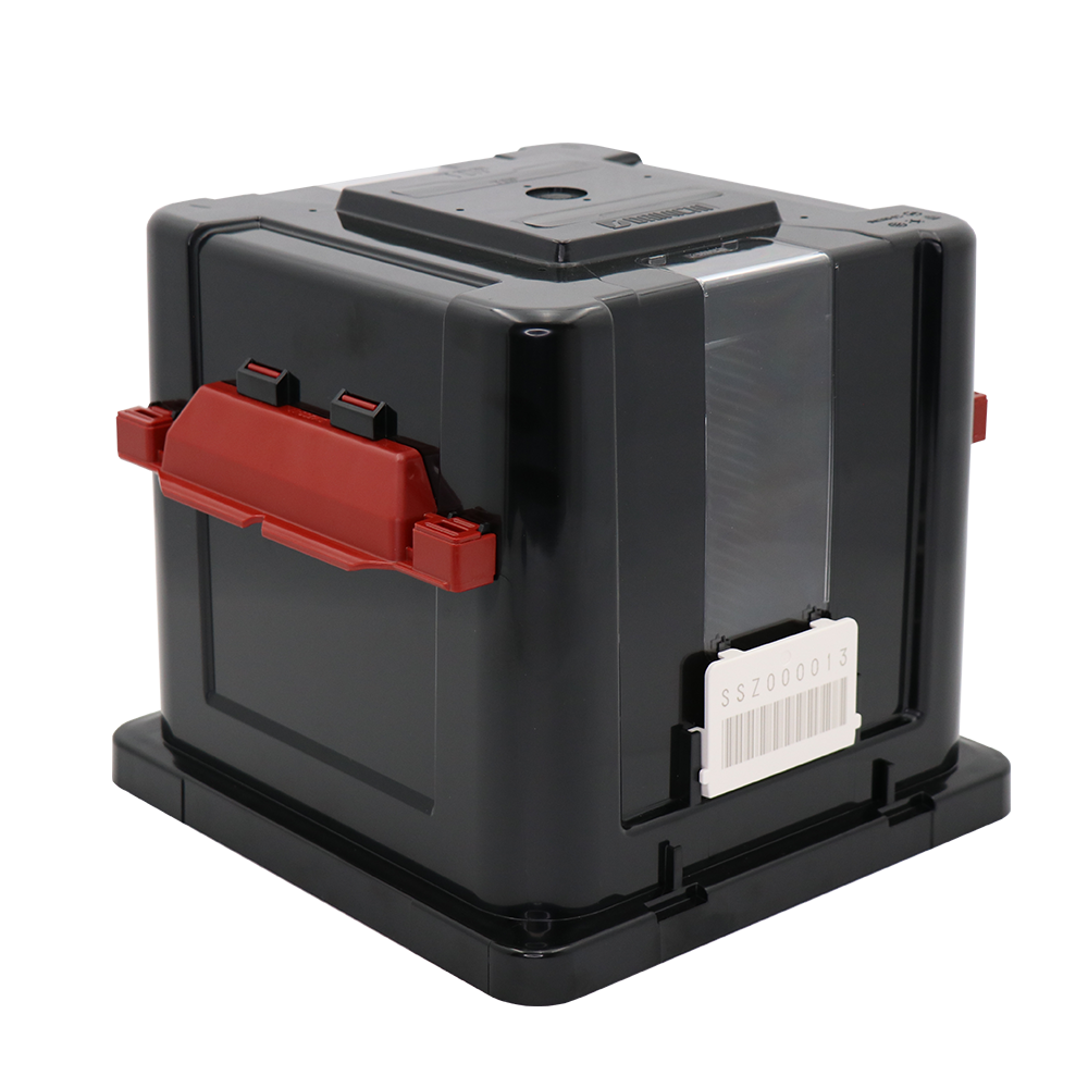
“I helped my customer by designing a process cassette that doubles as a shipping container. By creating this

solution, our customer was able to greatly increase efficiencies and scale production while improving yield.”

Alyssa Ellis
Account Executive

“During a customer review, we discovered photomasks were being over-packaged by the supplier. By simply specifying a smaller box, our customer saved space without spending a dime.”

Artemis Vasiliades
Account Executive

“I help customers optimize fab space by personally reviewing the storage and processing of critical devices and delivering complete solutions that include pre-programmed tracking tags, reticle pods, and custom cleanroom racks.”

Our flagship products

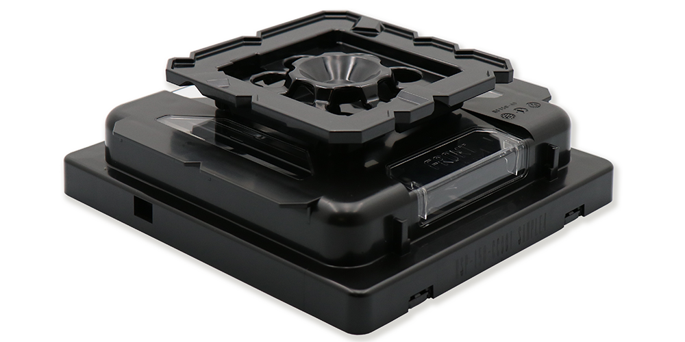
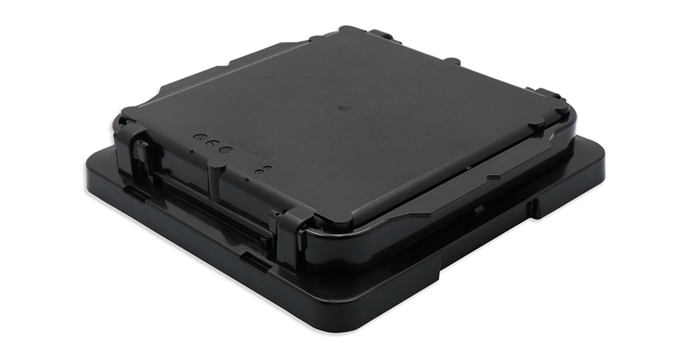
Pozzetta’s leading semiconductor device fabrication products are intuitively engineered, meticulously cleaned, and precisely designed to fit critical device standards and demands

Immaculate microcleaning methods

Pozzetta is also home to our class-6 cleanroom, providing complete incoming & pre-clean inspection, submicron cleaning with a purified water source, and 20,000 square feet of warehouse space through the semiconductor device fabrication and cleaning process.